
From wafer in to final test, the AWL series supports optical inspection throughout the semiconductor process flow.
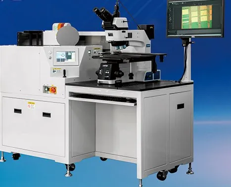
Compact wafer inspection stations built around the SOPTOP MX68R metallurgical microscope — automatic wafer boat scanning, notch / flat pre-alignment and front and back macro inspection.
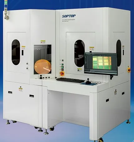
Fully enclosed EFEM system with dual-arm robot, FOUP loadports and non-contact pre-aligner, built on the SOPTOP MX12R. Choose manual (MS), fully automatic (AS) or linear-motor high-precision (RAS) stages.
Wafer handling, inspection, data and safety — engineered for production fabs.
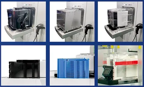
Flags tilted or misaligned wafers with alarms.
0°, 90°, 180° and 270° orientation settings.
Non-contact optical centre location.
Si · SiC · EMC · Glass
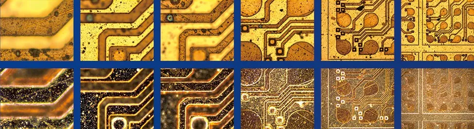
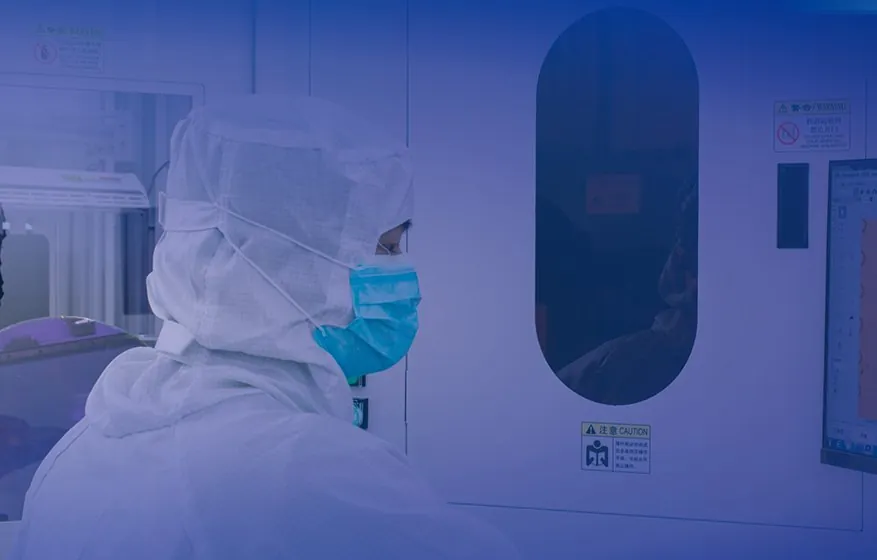
A fully automated wafer-handling system makes macro and micro inspection efficient. The AWL optical system captures fine micro detail in high definition, while a versatile macro module and an easy remote-control joystick enable multi-angle, full-field macro inspection — an efficient tool for wafer defect analysis.
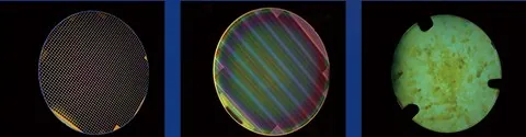
Sunny Instruments' own image-processing software drives the motorized stage, Z-axis, nosepiece and light source — compatible with 64-bit Windows and MX-series microscopes.
| Model | AWL046 | AWL068 |
|---|---|---|
| Wafer handling | ||
| Wafer size | 100 / 150 mm | 150 / 200 mm |
| Min. wafer thickness | 150 µm | 150 / 180 µm |
| Wafer carrier | Open cassette / SMIF pod | |
| Inspection mode | Full / odd-number / even-number inspection / manual selection | |
| Wafer boat scanning (yes / no / tilted) | ✓ | ✓ |
| Boat protrusion alarm | ≥ 4 mm | |
| Wafer pre-alignment (flat, notch) | ✓ | ✓ |
| Orientation setting | Non-contact positioning of flat and notch; 0°, 90°, 180°, 270° | |
| Inspection functions | Front macro (rotation); back macro 1 (outer ring, rotation); back macro 2 (center) | |
| Facility | ||
| Dimensions (W × D × H) | 1450 × 700 × 1600 mm | 1550 × 700 × 1600 mm |
| Power | 1P / 220 V / 10 A | |
| Gas (negative / positive pressure) | −70 kPa ~ −80 kPa / 0.5 MPa | |
| Optics | ||
| Microscope | SOPTOP MX68R metallurgical microscope | |
| Optical system | Infinity-corrected with aberration correction; 50× – 1000× | |
| Observation | Bright field, dark field, polarizing, DIC | |
| Eyepiece | High eye-point wide-field plan PL10×/22 mm, with reticle, diopter adjustable | |
| Viewing head | Hinged trinocular, 5 – 35° tilt, erect image; IPD 50 – 76 mm; two-stage split, binocular : trinocular = 100:0 / 0:100 | |
| Objectives | Long-WD plan BF/DF semi-apochromatic metallographic 5× / 10× / 20× / 50× / 100× | |
| Nosepiece | BF/DF 6-position electric nosepiece with DIC slot | |
| Frame | Reflected-light frame, low-position coaxial coarse / fine focus; coarse stroke 35 mm, fine accuracy 0.001 mm; anti-slip tension and upper-limit stop; built-in 100 – 240 V. BF/DF reflected illuminator with field diaphragm, electric variable aperture diaphragm, BF/DF switching, filter and polarizer slots; 12 V 10 W LED light box | |
| Stage | 6″ mechanical stage, low-position coaxial XY; wafer carrier Ø 38 mm, 360° rotatable; travel 228 × 170 mm; observation 170 × 170 mm; clutch handle | 8″ mechanical stage, low-position coaxial XY; wafer carrier Ø 60 mm, 360° rotatable; travel 280 × 210 mm; observation 210 × 210 mm; clutch handle |
| Other | Filter plate, polarizer / analyzer, DIC component, camera interface, adjustment platform, camera, professional wafer inspection software | |
| Model | AWL812-MS | AWL812-AS | AWL812-RAS |
|---|---|---|---|
| Wafer handling | |||
| Wafer size | 200 / 300 mm | ||
| Wafer thickness | 250 – 1000 µm / 300 – 1000 µm | ||
| Wafer carrier | FOUP, FOSB / SMIF pod / open cassette | ||
| Loadports | 1 port | 1 port / 2 ports | |
| Wafer boat scanning (yes / no / tilted) | ✓ | ||
| FOUP RFID reading | ✓ | ||
| Docking crane | — | Optional | |
| Robot | Dual-arm robot | ||
| Pre-aligner | Non-contact optical alignment | ||
| Wafer ID OCR | Optional | ||
| Macro inspection | Front macro (rotation); back macro 1 (outer ring); back macro 2 (center) | ||
| Macro inspection photography | — | Optional | |
| Macro light source (LED) | White, yellow and green light | ||
| Facility | |||
| Equipment weight | 1050 kg | 1350 kg | 1800 kg |
| Dimensions (1 port) | 2400 × 1400 × 2350 mm | ||
| Dimensions (2 ports) | 2400 × 2050 × 2350 mm | ||
| FFU | ✓ | ||
| ESD elimination | ✓ | ||
| UPS | Optional | ||
| Power | Single phase 220 V 50 Hz 16 A | Single phase 220 V 50 Hz 32 A | |
| Compressed air (CDA) | 0.4 – 0.6 MPa | ||
| Vacuum (VAC) | −70 kPa ~ −90 kPa | ||
| Optics | |||
| Microscope | SOPTOP MX12R metallurgical microscope | SOPTOP MX12RL metallographic illuminator | |
| Optical system | Infinity-corrected with aberration correction; 50× – 1000× | ||
| Observation | Bright field, dark field, polarizing, DIC | ||
| Eyepiece | High eye-point wide-field plan PL10×/25 mm, with reticle, diopter adjustable | ||
| Viewing head | Hinged trinocular, 0 – 35° tilt, erect image; IPD 50 – 76 mm; two-stage split, binocular : trinocular = 100:0 / 0:100 | ||
| Objectives | Long-WD plan BF/DF semi-apochromatic metallographic 5× / 10× / 20× / 50× / 100× | ||
| Focus | Manual focus | 5× auto pre-focus, optional real-time focus | Real-time focus |
| Nosepiece | BF/DF 6-position electric nosepiece with DIC slot | ||
| Frame | BF/DF reflected illuminator with field diaphragm, electric variable aperture diaphragm, BF/DF switching, filter and polarizer slots; 12 V 10 W LED light-source control unit | ||
| Stage | 12″ manual mechanical stage, low-position coaxial XY; wafer carrier Ø 70 mm, 360° rotatable; observation 305 × 305 mm; clutch handle | 12″ fully automatic stage, X / Y / Z / φ; wafer carrier Ø 70 mm, 360° rotatable; observation 310 × 310 mm; φ ±5°; high / low speed per axis | 12″ high-precision linear-motor automatic stage, X / Y / Z / φ; wafer carrier Ø 70 mm, 360° rotatable; observation 310 × 310 mm; φ ±5°; high / low speed per axis |
| Software & data | |||
| Wafer e-map with visual positioning | — | Optional | ✓ |
| Wafer review system | — | ✓ | |
| KLARF file import / export | — | ✓ | |
| Data communication (SECS/GEM) | Optional | ✓ | |
| Other | Filter plate, polarizer / analyzer, DIC component, camera interface, camera, professional wafer inspection software | ||
Share your wafer size, carrier type and automation level — we'll recommend the right AWL configuration.
Request a quote