Nexa Beyond
ENTH
Home
Products
SOPTOP Industrial Microscopes Material Science Microscope Life Science Microscope Nano Surface Analysis (SEM) 3D Portable Imaging Thermal Analysis Endurance & Mechanical Testing Smart Display Microscope
Company
Image Gallery Blog About us Contact us
Home/Products/Nano Surface Analysis
CIQTEK Electron Microscope

Nano Surface Analysis with Scanning Electron Microscopy

Scanning Electron Microscope and Atomic Force Microscope solutions from CIQTEK — from tungsten-filament SEM to Field-Emission and Focused Ion Beam systems, resolving structures down to 0.6 nm.
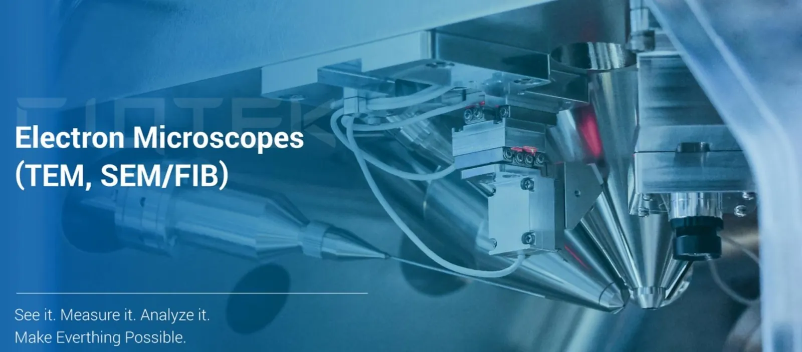
CIQTEK Electron Microscopes TEM SEM FIB

Tungsten Filament SEM

W SEM
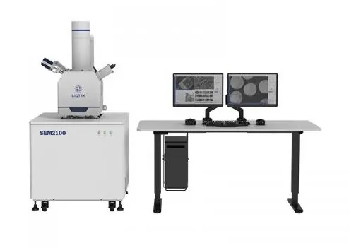
CIQTEK SEM 2100

SEM 2100

TUNGSTEN FILAMENT · SE / BSE / EDS

A dependable entry into electron microscopy delivering high-contrast imaging for routine analysis, education and quality control.
Magnification
1 – 300,000×
Detectors
SE · BSE · EDS
Resolution (SE)
3 nm @ 20 kV
Resolution (BSE)
4 nm @ 20 kV
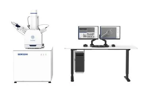
CIQTEK SEM 3200

SEM 3200

TUNGSTEN FILAMENT · LOW-VACUUM CAPABLE

Adds a low-vacuum mode for non-conductive and outgassing samples, with excellent low-kV performance for surface-sensitive imaging.
Detectors
SE · Low-vac · BSE · EDS
Resolution (SE)
3 nm @ 30 kV
Low-kV (SE)
7 nm @ 3 kV
Low-vac (SE)
3 nm @ 30 kV · 30 Pa
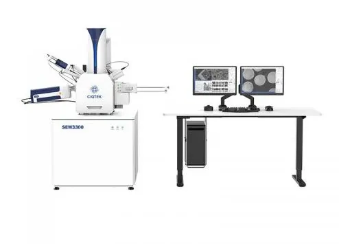
CIQTEK SEM 3300

SEM 3300

TUNGSTEN FILAMENT · IN-LENS DETECTION

A high-performance tungsten system with In-lens detection for superior low-voltage resolution and fine surface detail.
Detectors
SE · In-lens · BSE · EDS
Resolution (SE)
2.5 nm @ 15 kV
Low-kV (SE)
4 nm @ 3 kV
Ultra-low kV
5 nm @ 1 kV

Field Emission SEM

FE SEM
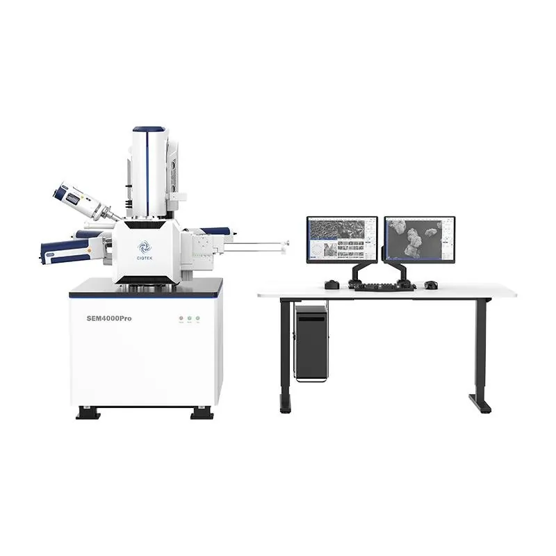
CIQTEK SEM 4000Pro Field Emission SEM

SEM 4000Pro

FIELD EMISSION · ANALYTICAL PLATFORM

A versatile analytical FE-SEM supporting a full detector suite for morphology, composition and crystallography in a single platform.
Magnification
1 – 1,000,000×
Detectors
SE·BSE·EDS·Low-vac·EBSD·STEM·CL
Resolution (SE)
0.9 nm @ 30 kV
Low-vac (SE)
1.5 nm @ 30 kV · 30 Pa
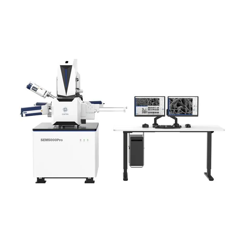
CIQTEK SEM 5000Pro Field Emission SEM

SEM 5000Pro

FIELD EMISSION · HIGH RESOLUTION

Ultra-high resolution with In-lens detection and 2.5 million× magnification for the most demanding nano-characterization.
Magnification
1 – 2,500,000×
Detectors
SE·In-lens·BSE·EDS·EBSD·STEM·CL
Resolution (SE)
0.7 nm @ 15 kV
Low-kV (SE)
1.1 nm @ 1.0 kV
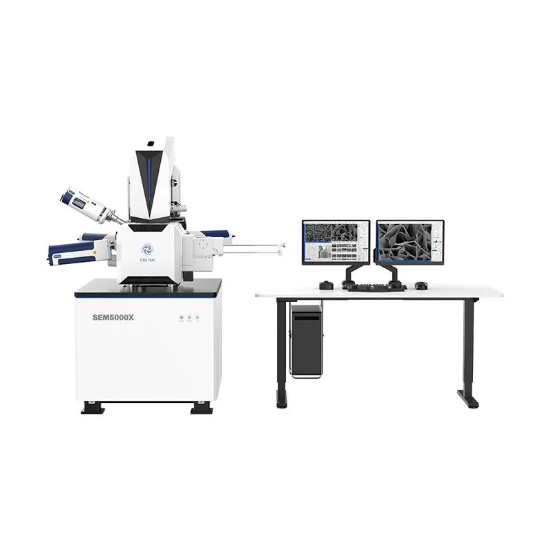
CIQTEK SEM 5000x flagship FE-SEM

SEM 5000x

FIELD EMISSION · FLAGSHIP

Our finest resolving power — 0.6 nm at 15 kV — engineered for cutting-edge research in semiconductors, energy materials and life sciences.
Resolution (SE)
0.6 nm @ 15 kV
Low-kV (SE)
1.0 nm @ 1 kV
SemiconductorsEnergy materialsLife science

Focused Ion Beam SEM

FIB SEM
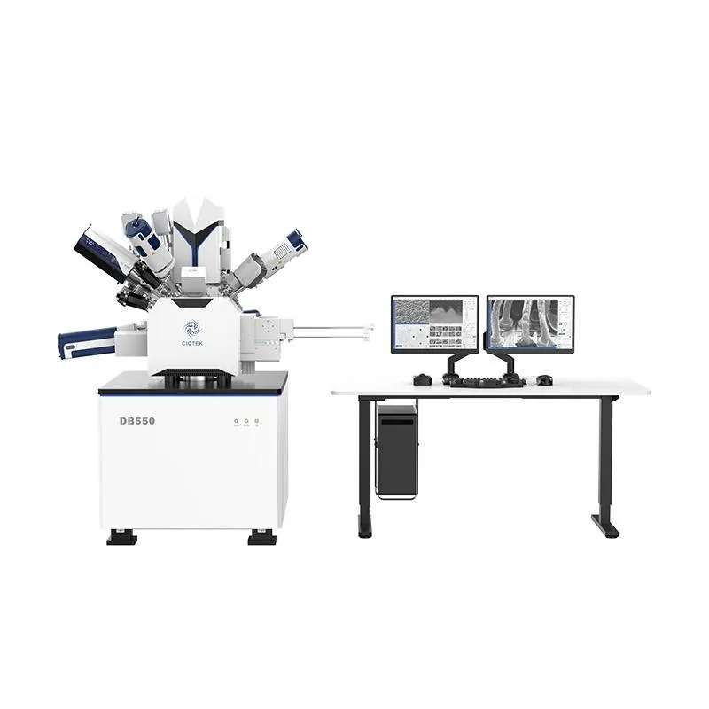
CIQTEK DB550 Dual Beam FIB-SEM

DB 550

DUAL BEAM · ELECTRON + GALLIUM ION

A dual-beam platform combining electron imaging with a gallium ion column for precise cross-sectioning, TEM lamella preparation and 3D nano-machining.

Ion source
Gallium
Ion resolution
3 nm @ 30 kV
Acceleration
0.5 – 30 kV
Option
Nano-manipulator
Gas Injection SystemPlasma CleanerCross-sectionLamella lift-outTEM prep
Imaging examples

Seeing the invisible

Real micrographs captured on CIQTEK electron microscopes across materials and life science. Click any image to view it larger.
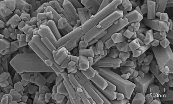
SEM micrograph of crystalline rods
Crystalline material500 nm
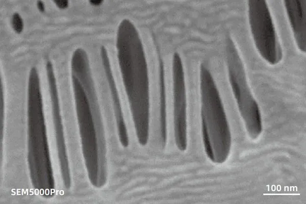
SEM micrograph of mesoporous membrane
Mesoporous membrane100 nm
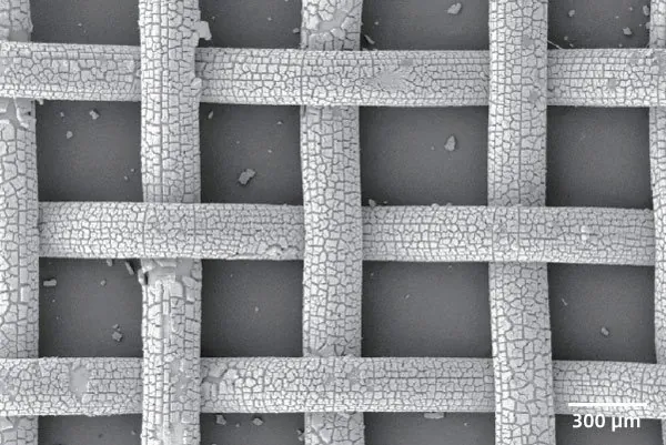
SEM micrograph of mesh grid
Mesh structure300 μm
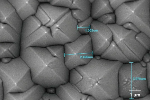
SEM micrograph of crystalline film
Crystalline film1 μm
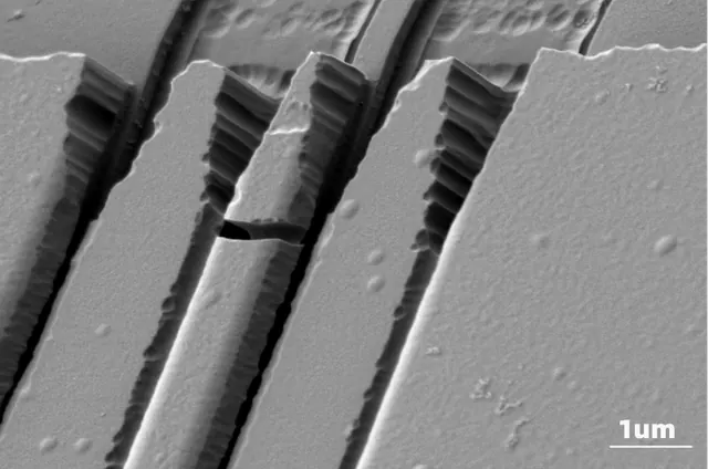
SEM micrograph of waveguide cross-section
Waveguide1 μm
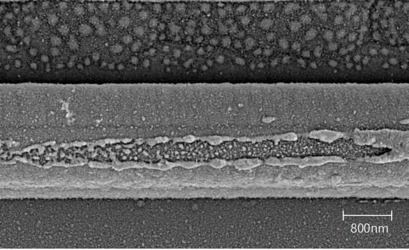
SEM micrograph of nanowire fiber
Nanowire / fiber800 nm
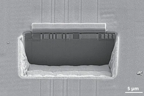
FIB-milled chip cross-section
FIB chip cross-section5 μm
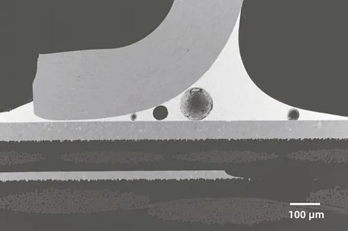
FIB particle cross-section
FIB particle cross-section100 μm
FAQ

Frequently asked questions

What is the difference between a tungsten SEM and a field-emission SEM?

Tungsten-filament SEMs such as the SEM 2100 are a dependable, cost-effective choice for routine imaging and QC. Field-emission SEMs reach far higher resolution — the SEM 5000x resolves 0.6 nm at 15 kV — for demanding nano-characterization.

Can I image non-conductive samples?

Yes. The SEM 3200 includes a low-vacuum mode for non-conductive and outgassing samples.

Can CIQTEK SEMs analyze composition?

Yes. Systems can be equipped with detectors such as EDS for elemental analysis; the SEM 4000Pro supports a full detector suite for morphology, composition and crystallography.

What is a FIB-SEM used for?

The DB 550 dual-beam system combines electron imaging with a gallium ion column for precise cross-sectioning, TEM lamella preparation and 3D nano-machining.

Bring your samples into focus

Our specialists will help you choose the right SEM configuration for your resolution, throughput and budget.

Request a consultation